 Fraunhofer Institute for Electron Beam


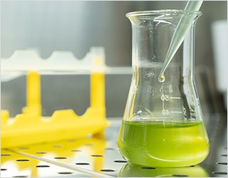
The Fraunhofer Institute for Electron Beam and Plasma Technology FEP has received regulatory approval to conduct activities at biosafety level 2. The laboratory complex thus opens up new research and testing opportunities for industry and project partners. This approval marks an important milestone in the development of the institute’s biomedical laboratory unit.
more info